3d dram admnd tsv differences
Pairs 4 Gbs per pair Co-developed with. Qualcomm Near Future 2014 -2017.
3d Ic Technology And Reliability Challenges By Samiksha Jadhav 3d Ics Medium
To meet the performance requirement 3D chip stacking using Through-Silicon-Via TSV has been developed in recent years.

. The semiconductor industry is actively pursuing 3D Integrated Circuits 3D-ICs with Through-Silicon Via TSV technology Fig. Cannot accurately capture the faulty behavior of TSV open defects in 3D DRAM. DATE is successfully validated against several commodity planar and 3D DRAMs.
As shown in Fig 8b the International Technology Roadmap for Semiconductors ITRS projects TSV pitch remaining in the range of several microns while on-chip interconnect pitch is in the range of 100nm. For 25D interposer 3D IC. DATE provides front-end and back-end DRAM process roadmap from 90 nm to 16 nm node and provides a broader range 3D DRAM design model along with emerging transistor device.
To order 3-D DRAM Stacked TSV System Chips October 2014. TSV utilized for DRAM Stack and Memory Controller 256 GBs peak DQ bandwidth across 800 diff. RTI International 9 3D ASIP Dec.
850 if a Memory Technology Report has been ordered from Memory Strategies in the past year. Logic and their RDL needs. For TSV technology devices are connected by short vertical through-wafer via and thus enhance the.
2014 Interposer products Wide IO DRAM mobile Far future 2017 -2025 Beyond CMOS photonics sensors etc Source. A double-sided IC package with a memory controller and 3D-stacked DRAM A 3D silicon interposer with double sided RDL layers and active dies on both sides Compare and contrast these technologies. A edge memory non-center logic b center center c edge.
Also by increasing the number of stacked layers from eight to 12 Samsung will soon be able to mass produce 24-gigabyte GB High Bandwidth Memory which provides three times the. Send us the information requested below by e-mail fax or post along with your check bank transfer or purchase order for 975. Right- IBM embedded DRAM with Cu TSVs.
Die size difference die thickness etc. Download scientific diagram TSV locations in 3D DRAM vs. Relying on its 12-layer 3D-TSV technology Samsung will offer the highest DRAM performance for applications that are data-intensive and extremely high-speed.
In addition as the coupling effects between aggressor TSVs and victim TSV vary with the op-eration of the DRAM the faulty behavior of TSV open de-fects in 3D DRAM is affected by many factors eg opera-tion type ie read or write voltage of its neighboring word-. As CPU performance has continually enhanced by transistor scaling the demand in DRAM performance has been also increased. The TSV pitch will not.
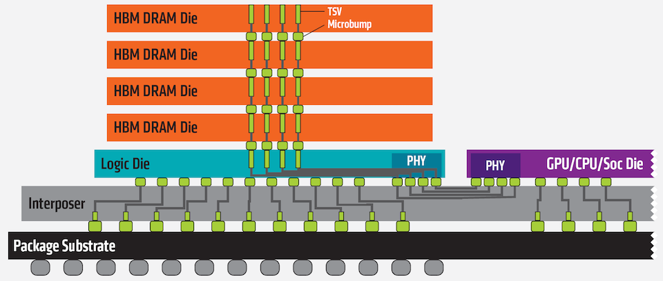
3D stacking of DRAM dies on a processor core and connected by TSVs can yield massive inter-die bandwidths and dramatic reductions in access latency. RTI International 27 3D ASIP Dec. 10-12 2014 TSV for Interposers and 3DIC Implementation differences for Si interposer Vs.
Level DRAM Area Timing and Energy model DATE which supports 3D DRAM design with TSV. We investigated different DRAM families WIDE IO DDRSDR LPDDR and LPDDR2 and densities that range from 256Mb to 4Gb per channel. Most prior research on 3D processor-DRAM inte-gration featured several conventional commodity 2D DRAM dies stacked as main memory1-3 Loh for example4 demonstrated that the performance of 3D processor-DRAM integrated systems could be further improved through Tezzaron Semiconductors non-conventional so-called true 3D DRAM.
2013 Atotech Spherolyte III. European 3D TSV Summit Jan. TSV technology and challenges for 3D stacked DRAM articleLee2014TSVTA titleTSV technology and challenges for 3D stacked DRAM authorChang Yeol Lee and Sungchul Kim and Hongshin Jun and Kyung Whan Kim and Sung Joo Hong journal2014 Symposium on VLSI Technology VLSI-Technology.
Contact Memory Strategies or. The memory wall has been a topic for some time due to limited IO bandwidth and power consumption constraints. Using a capacitorless 1T DRAM cell architecture.
The implementation results of the proposed 3D-DRAM subsystem. Current High Density 25D3D TSV Applications and Outlook Source.

3d Stacked Dram Example High Bandwidth Memory Consists Of Stacked Download Scientific Diagram

A 3d Packaging Technology For High Density Stacked Dram Semantic Scholar
3d Ic Technology And Reliability Challenges By Samiksha Jadhav 3d Ics Medium

3d Layer Stacking Tsv Technologies Set To Refresh Memory

Samsung Develops First 12 Layer 3d Tsv Chip Packaging Technology Cdrinfo Com

3d Stacked Dram Example High Bandwidth Memory Consists Of Stacked Download Scientific Diagram

3d Stacked Dram Example High Bandwidth Memory Consists Of Stacked Download Scientific Diagram

3d Stacked Dram Example High Bandwidth Memory Consists Of Stacked Download Scientific Diagram

Samsung 3d Tsv Stacked Ddr4 Dram I Micronews

3d Stacked Dram Example High Bandwidth Memory Consists Of Stacked Download Scientific Diagram
Ddr4 Prepare To Get Mugged By Your Supplier Insignis Technology Corporation Insignis Technology Corporation

3d Integration By Tsvs A Scanning Electron Microscope Sem Image Of Download Scientific Diagram
Advanced Semiconductor Packaging Starting To Change Memory Market Landscape Seeking Alpha
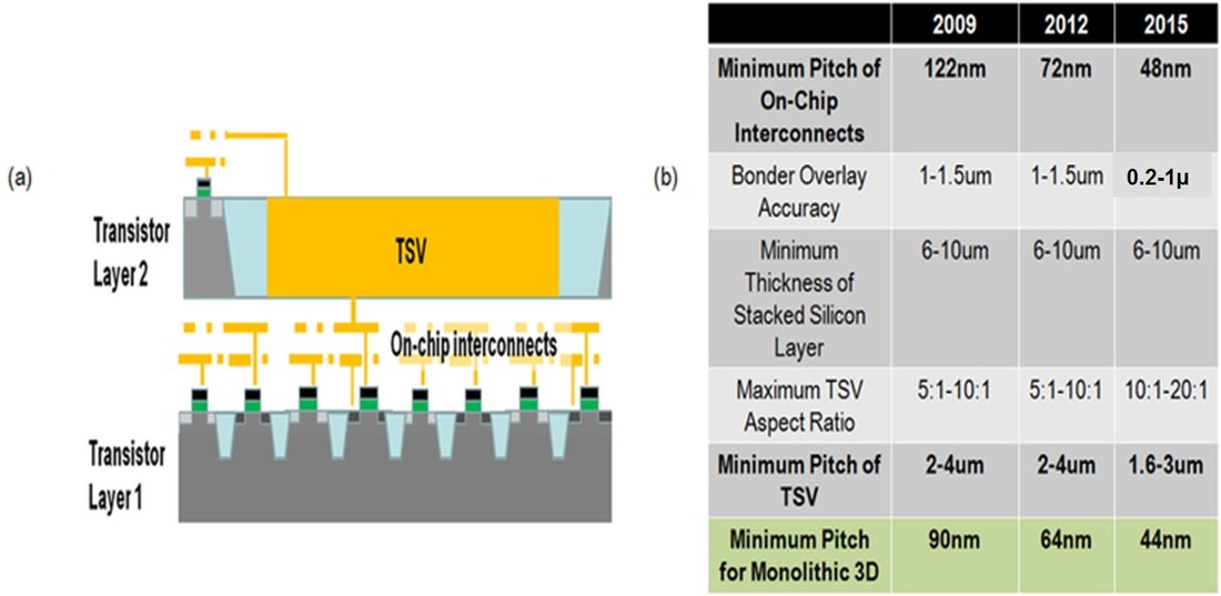
Tsv Vs Monolithic 3d

The Floorplan Of 3d Swift A Sub Bank Consists Of 32 Mats And Each Mat Download Scientific Diagram

An Exact Measurement And Repair Circuit Of Tsv Connections For 128gb S High Bandwidth Memory Hbm Stacked Dram Semantic Scholar
3d Stacked Dram Example High Bandwidth Memory Consists Of Stacked Download Scientific Diagram

Pdf 3d Stacked Memory Architectures For Multi Core Processors Semantic Scholar
Choosing Between Ddr4 And Hbm In Memory Intensive Applications Tech Design Forum Techniques